A History of the PC's BIOS
Why spend any time at all studying or even briefly reviewing the history of BIOS code, rather than jumping right into the latest UEFI firmware (boot) code?! Because it's only by having at least some understanding of the relatively intricate (for its time) contents of what can now be called archaic Legacy BIOS code, that one can truly appreciate how incredibly complex BIOS code soon became![1]
Introduction
It would take a group of accomplished authors working full-time to produce a textbook on the complete history of the PC BIOS in a reasonable
amount of time. It will take us much longer to even produce a brief summary of how PC BIOS code has changed over the years. Though we have provided many
details on special topics (such as Checksum Bytes and even some assembly listings), we are limited in the research we can conduct and the access we have to
different types of computers. Nevertheless, we hope to provide some data on this subject you may not find elsewhere.
What should set this page apart
from most others discussing PC BIOS history are its DEBUG examples and hands on Lab work which I hope the majority of my readers will not only study but
carry out for themselves to further their understanding.
The Term "BIOS"
Years before the IBM (5150) PC project was proposed; although the IBM 5100 can in some ways be thought of as the PC's forerunner, the term BIOS was used by Gary A. Kildall by at least 1975 (the proof being in the assembly source code for his BDOS file[2]). After having supplied Intel with a PL/M compiler and other products for their Intelec 4 and 8 Development Systems, Kildall perfected his CP/M OS and BIOS code apparently on an Intel MDS-800 Microprocessor Development System;[3] which coincidentally, may have been the same type of system used by Dave Bradley to develop the BIOS code for the IBM PC. Bradley wrote on July 27, 2021, in a reply on this webpage (concerning a 2014 article, "The IBM PC BIOS and Intel ISIS-II"), "It was indeed assembled on an Intel MDS using ASM86. I have no recollection of models or version numbers. It was developed in individual modules, but I put them all into a single source file for publication in the TRM [Technical Reference Manual]."
What a BIOS Does
Though the details of various BIOS functions (and their order) have changed; along with many new functions being added over the years, this is a list of the fundamental operations which the BIOS (Basic Input/Output System) code either must or only might complete before handing control over to an operating system. Due to the increased complexity of even decades old BIOS code, completing these items came to be known as the POST (Power On Self Test), since the BIOS also contained code for many other tasks (such as routines for changing settings in BIOS CMOS Memory and other features):
- Test the Processor (CPU)
- Verify its own code using checksums
- Test Memory; may be preceded by DMA (Direct Memory Access) testing
- Test the Controller chips on the Motherboard
- Test that CPU Interrupts can be processed correctly
- Test and Initialize I/O Interfaces; identify any media drives connected
- Test any Serial port devices
- Identify any 'Option ROM' devices with BIOS code of their own
- Verify any Option ROM code using checksums
- Allow such devices to run their own BIOS code and return
- Initialize the BIOS Data Area in Memory
- Test for indications of an OS Loader on any media
- Pass control of the PC to that code
As can be seen from the partial list above, a computer's BIOS is inextricably linked to its hardware. Therefore a history of the BIOS code must also include at least an historical summary of changes in PC hardware. Before computers with modern processors and other internal devices, advanced types of memory, etc. ever became available to the public, they invariably required changes in the BIOS code. It's important to note the major differences (such as, bus width and addressable memory) in the Intel® processor family (see table below) for any historical study of the PC's BIOS.
A Few Relevant Facts concerning some early Intel® Processors | |||||
Processor ( |
Bits per Bus |
Addressable Memory |
Initial Clock Speed |
Introduced |
|
Data |
Address |
||||
8 |
16 |
64 KiB |
2 MHz |
April 1974 |
|
16 |
20 |
1 MiB |
4.77 MHz |
June 1978 |
|
8 |
20 |
1 MiB |
4.77 MHz |
July 1979 |
|
16 |
20 |
1 MiB |
6 MHz |
JAN 1982 |
|
8 |
20 |
1 MiB |
6 MHz |
JAN 1982 |
|
16 |
24 |
16 MiB[4] |
6 MHz |
FEB 1982 |
|
32 |
32 |
4 GiB |
16 MHz |
OCT 1985 |
|
Except for some early notebook CPUs (e.g., ![]() 386SX), all Intel processors from 80386
and later, such as the
386SX), all Intel processors from 80386
and later, such as the ![]() 80486 (late 1989), were capable of addressing 4 GiB of Memory. But the maximum amount of memory an i486 through
6th-generation CPU based PC (i.e., Pentium™ Pro/-II/-III and Celeron™) could actually use was often
determined by the Memory Control chips available to motherboard manufacturers. For example, a particular
ASUS™ motherboard (CUSL-2C); circa 2000, designed for Socket 370 Pentium™ III or Celeron™ processors, only
supported up to 512 MiB[5] (even though CPUs which could access at least 4 GiB had been
available for 15 years) due to the limitations of its MCH (Memory Controller Hub).[6]
80486 (late 1989), were capable of addressing 4 GiB of Memory. But the maximum amount of memory an i486 through
6th-generation CPU based PC (i.e., Pentium™ Pro/-II/-III and Celeron™) could actually use was often
determined by the Memory Control chips available to motherboard manufacturers. For example, a particular
ASUS™ motherboard (CUSL-2C); circa 2000, designed for Socket 370 Pentium™ III or Celeron™ processors, only
supported up to 512 MiB[5] (even though CPUs which could access at least 4 GiB had been
available for 15 years) due to the limitations of its MCH (Memory Controller Hub).[6]
The advent of 64-bit processors meant computers might possibly access up to 16 EiB (16 Binary Exa Bytes) of memory at some point in the future. However, all 7th and 8th-generation 64-bit CPUs have been manufactured with far less than 64-bit address lines; 36-bit (for 64 GiB) and now 40-bit (for 1 TiB) are common. As noted above, a PC's chipset (such as its MCH) has often been the limiting factor regarding memory; and is still often true. For example, a GIGABYTE™ GA-G33M-DS2R from 2007, with an LGA775 socket for many different Intel 64-bit CPUs, only supported up to 8 GiB[7] of system memory due to the limitations of its 82G33 Graphics and Memory Controller Hub (GMCH).[8]
Of course, in order to generally make use of more than 4 GiB of RAM, a 64-bit OS is also needed. (Note: PCs with 32-bit OSs often show only about 3.2 to 3.3 GiB available when 4 GiB is installed, since addressable hardware; especially onboard video controllers, may use hundreds of MB for their own support.)
We will have more to say about how BIOS code was affected by changes in the amount of memory these processors could access.
The IBM PC BIOS Code; Clones, Lawsuits and Compatibles
IBM published the full source code for the BIOS of all of their early PCs. The code is quite easy to find online from various sites today; both in PDF copies of the early Technical Reference manuals (e.g., here's a copy of the IBM 5150 Technical Reference manual; PDF pages "193/393" and following contain the BIOS ROM code listing) and as files containing the actual binary bits extracted directly from the old BIOS chips. In fact, some emulators, such as PCE, actually make use of the original BIOS and ROM BASIC code which is why we can reproduce this error in the first ROM BASIC version. It must be noted that there were at least three "personal computers" available to the public prior to the IBM PC: The Apple II and the Commodore PET (April, 1977, both 6502 CPU based); which actually made use of the term personal computer, and then the TRS-80 (August, 1977, using a Zilog Z80 CPU). Of the three, only Apple published its BIOS code; though later on books by independent authors on the ROM BASIC code of the TRS-80 became available.[9]
In less than a year after release of the IBM PC in 1981, both Eagle Computer and Corona Data Systems created IBM PC Clones which eventually led to them being sued by IBM early in 1984. Eagle was forced to stop production until eventually rewriting their BIOS. But in the meantime, PC Compatibles such as COMPAQ (using legally designed compatible BIOS code) had far outpaced them. Unable to regain enough sales, Eagle went out of business in 1986. Corona met a different fate: Its founder, Robert Harp, resigned in 1987, after the Daewoo Group acquired 70% of Corona, and by 1993 it was completely phased out. However, in June 1982, Columbia Data Products created the first legally PC compatible BIOS[10] for their MPC 1600, and in November 1982, came the announcement of Compaq's legally engineered BIOS,[11] which cost them a Million Dollars! Then in May, 1984, Phoenix Technologies became the first company to announce that they had created a PC compatible BIOS for sale to any PC / motherboard manufacurer. I recommend reading all of this article by the one who wrote that BIOS code and then his How the First BIOS Code was Written article which delves more into the details of BIOS code writing. In 1985, yet another company, DTK Computer, decided to develop its own clean-room PC BIOS.
Following the creation of the Phoenix BIOS, Award Software slowly became a noticeable competitor in the BIOS code market. But, in 1998, it was merged into Phoenix Technologies. The only other major BIOS company, AMI (American Megatrends, Inc.), began producing BIOS software in 1986, among its other products; including motherboards, helping to keep them solvent to this day. They did have some "technical problems" over the decades, such as the "Happy Birthday Trojan" (though that term may not be quite accurate), which on November 13, 1993, caused many PCs with a particular BIOS chip to halt at boot-up and repeatedly play the happy birthday tune through the PC's speaker. However, they are still producing and selling BIOS code with competitive features: Some fairly recent products from Gigabyte Technology (which used Award BIOS in the past) now have UEFI code by AMI in them (e.g., in a 256 Mbit GigaDevice 25Q Series flash chip on their B460M DS3H motherboard).
Programs had Easy Access to BIOS code in the Past
First, some necessary background: For many years after the first IBM PC was shipped, a number of routines in the PC's BIOS code were absolutely critical for every single application or utility program that ever ran under IBM PC DOS or MS-DOS. Assembly code for all such early x86 programs contain what are still called Interrupts for accessing keyboards, Memory, Video routines for the display, floppy drives, speakers and other peripherals. From the beginning, DOS had its own Interrupt calls as well (for both BIOS and DOS Interrupts, see Ralf Brown's Interrupt List), but as operating systems grew, their developers created more code that ran in between applications and the BIOS code. Eventually, modern OS code, replaced most BIOS Interrupts through the use of what came to be known as drivers, allowing them access to the hardware apart from any BIOS code; increasing the layers between application code and the hardware. However, until that occurred, there were dedicated Memory bus locations that any program could use to by-pass an OS and hand control over to BIOS Interrupt code; for example, to get input from the keyboard or write directly to Memory locations used by a monitor for what was displayed on its screen (or any other hardware that had specific bus output PORTs on the system)!
In the beginning, these Memory (or bus PORT) locations were hardwired to the BIOS chips (via physical Memory address lines in the PC) and were directly accessed by using specific CPU commands. Of the maximum of 1 MiB of memory which the first PC's CPU (an Intel 8088) could possibly access, the highest "Memory Address" lines (0xF6000 through 0xFFFFF; exactly 40 KiB;) were connected directly to the BIOS and ROM BASIC chips (the BIOS using only the highest 8 KiB). Thus, for many early versions of DOS, one could quite easily make a binary copy of the whole BIOS using the DEBUG utility to save it to a file! As an example, if you boot an IBM PC (or a true IBM PC emulator) with a 5150 BIOS chip, and have at least 8 KiB of space on a diskette (we'll use the B: drive here for that), you can copy that PC's BIOS contents to the file DUMPBIOS.BIN by executing the following:
Enter today's date (m-d-y): 04-08-2023 |
The contents of the DUMPBIOS.BIN file will be identical to the bytes copied by some other means directly from the BIOS chip. DEBUG could also be
used to copy the IBM BASIC code from its ROM chips: For the BASIC ROM chips in a 5150 PC, you could name the output file "DUMPBAS.BIN" and in the
M command, simply substitute "M F000:6000 L 8000 100" for what you see above. You would also need to use a size of 8000 in the rcx
command. That will copy all 32 KiB (0x8000) from Memory locations F000:6000 (or 0xF6000) through F000:DFFF (or 0xFDFFF); a length of 0xE000 - 0x6000 = 0x8000 bytes.
After comparing DUMPBAS.BIN to a known good and verified ROM file, they were identical. It's a known fact, that for all early IBM PCs and compatibles; though
one must be aware of the size and layout of the BIOS code, that identical copies of the ROM chips can be created using DEBUG (or a similar utility) without having
to disassemble a PC, remove the chips and read their contents using some electronic device. Although most IBM XT computers have two 32 KiB BIOS chips inside them, only the highest 8 KiB of U19 comprise the BIOS code, so the same steps above could
be used to copy its BIOS code (see here for pictures and a list of
all the different IBM XT BIOS revisions).
In order to compare the contents of the two BIOS chips from
an IBM PC/AT (5170) (80286 CPU) to a file created by DEBUG, one must
first combine the "even" bytes of its U27 chip with the "odd" bytes of its U47 chip;[12] well, unless you
already have access to such a file. Then, in DEBUG; most likely under IBM PC DOS 3.30, since these chips total a length of 64 KiB and DEBUG can only work with
files up to 64 KiB minus 256 (0x100), the copy process must be broken into two parts: At the DEBUG prompt, after entering the first filename (which we'll
name BIOSDMP1.BIN with the N command), enter: M F000:0,FEFF 100, then set the size to FF00 using the rcx
command, followed by w to write 65,280 bytes to that file. Next, write the remaining 256 bytes to BIOSDMP2.BIN (which can be done in the same DEBUG session
after using another N command for the new file) then entering: M F000:FF00,FFFF 100 with an RCX of only 100
followed by the w and q commands. Lastly, combine the two files using the COPY command like this: COPY /B BIOSDMP1.BIN+BIOSDMP2.BIN
DUMPBIOS.ROM. Upon comparing DUMPBIOS.ROM with the bytes taken directly from the two BIOS chips, they are found to be identical.
However, for many decades now, there has generally been no way for an operating system or its applications, to directly access a BIOS chip's contents. Some motherboard manufacturers have provided customers with specialized utility programs to make backup copies of the BIOS code, but this is nothing like being able to divert full control of a PC to the BIOS code from inside an application as one could do in the early days of DOS (for example, it was possible to enter a single command in DEBUG which would reboot the PC in much the same way as pressing the CTRL + ALT + DEL keys did back then! At a DEBUG prompt, that command is: "g = f000:fff0", or: "g = ffff:0"). This should work under any DOS emulation or virtual machine. But attempting to do so under any Windows NT or XP OS will simply stop the DEBUG program.
Note: It must be pointed out that the simplest features computer users take for granted today, such as a
Real-Time Clock (or RTC), did not exist in the first IBM PC. Thus the reason IBM PC DOS 1.00
and 1.10 required users to enter the date and time! Nor did the BIOS automatically configure
such things as the amount of Memory in a PC; which required settings to be made using physical switches inside the chassis. Even the IBM PC/AT with an
80286 CPU and an RTC installed needed to use a Diagnostics diskette to SETUP the PC; easy to access BIOS Setup screens did not exist until
after some PC Compatible BIOS code included them:
 | The 80286-based IBM PC/AT required users to run a SETUP diskette the first time the PC was powered-on in order to store the time & date and hardware configurations; such as the number of disk drives on the system in its CMOS. Changing hardware, such as a disk drive, or having the CMOS battery die, also required using the SETUP diskette again. |
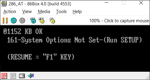
Some VM Labwork (using 86Box):
There are some Virtual Machines which have been created to actually try to emulate all the firmware code of a PC; not to simply make it possible to run old OS code. PCem and 86Box are two such projects. Click on the following link to learn how to install WinBox for 86Box, and then use an image file of an original IBM Diagnostics diskette to step through setting up the BIOS CMOS Memory of an IBM PC/AT.
BIOS Shadowing and Relocation
What is BIOS shadowing? A simple definition from Phoenix Technologies:
- "Shadowing / A technique
for improving the speed of ROM-based code. The code is copied from ROM to high-speed RAM at the same address, the ROM is disabled, and the RAM is then
write-protected."[13]
And a definition for the related topic of:
- "Memory Relocation / A technique for redefining redundant RAM memory as extended memory. Some systems contain both ROM
and RAM at the same addresses in the range A0000h - FFFFFh, with one or the other disabled. If this address range is not used for EMS or shadowing, the RAM's
upper address bits can be set to effectively relocate it to the top of the system's address space."[14]
But making a useful copy of a PC's BIOS from ROM into RAM required more than just a new routine in the code! Note carefully those words above about disabling the ROM and then write-protecting some of the RAM. That couldn't be done until changes were made in the chips; so new hardware had to be designed to carry out those functions. Chips and Technologies (in 1987) was the first company to create a full chipset which allowed BIOS code to implement shadowing — that chipset being trademarked as NEAT ("New Enhanced AT"). However, the company and PC which highly likely was the very first to use BIOS shadowing (though not by that name) was the COMPAQ DeskPro 386 which was available in September of 1986.
More notes on this will follow, but I wanted to be sure to point this out ASAP.
Note: There is much more I need to add with references concerning both of these topics. I will also be adding another page of instructions on installing and using the emulator 86Box (based upon PCem). If you need to know more about these topics now, you can email me here.
More Virtual Machine Labwork:
Install either VMware Player (see item # 1 under Replacing the VMware BIOS below) or Oracle VM VirtualBox or both. If you do decide to install both, I highly
recommend using VMware Player as your primary virtual machine, and do not install any networking for VirtualBox.
You may also have some conflicts with USB adapters, etc. when running both a VMware VM and VirtualBox at the same time. Some important quick
help: Once you click your mouse cursor inside any VMware virtual machine window, to get it back again for use with your Host OS,
you must press both the CTRL and ALT keys at the same time! Under VirtualBox, you must press only
the CTRL key on the right side of the keyboard.
The first VM I'd recommend creating would be MS-DOS 6.22; if you
don't have your own disk images, you can download them inside a .7z
file from here; with SHA1 hashes to check each diskette image file! (Download free 7-Zip program
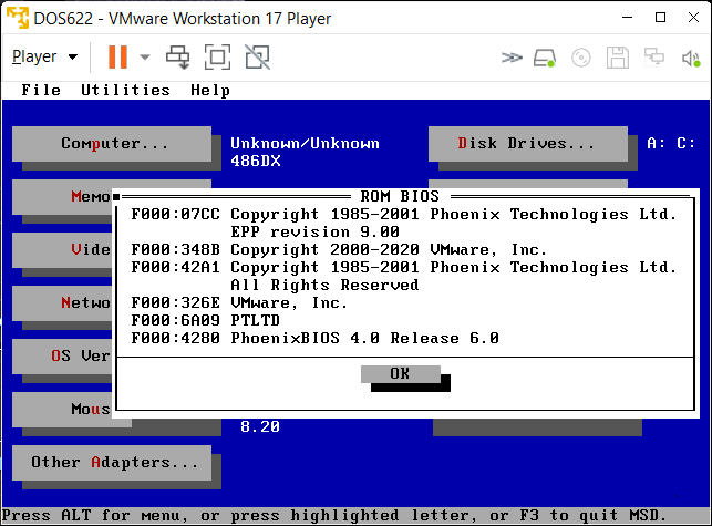
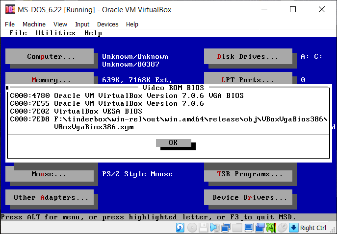
from here.) For whichever VM you're running, execute the DEBUG command I wrote about above. After that, enter msd at the DOS prompt and under the "Utilities" menu, choose "Memory Browser ..." and select each of the choices ("ROM BIOS", "Option ROM" and "Video ROM BIOS") to
reveal some of the strings you'll find inside that VM's DOS compatible BIOS code. Here is an example from each VM:
And for those addicted to using a mouse cursor, I've created a diskette image file with a mouse.com mouse driver
you can run under DOS; along with some other useful utilities, so download tsrutils.zip now,
connect the floppy image under your DOS VMs, copy mouse.com and mouse.ini to your
C:\ drive (or C:\DOS directory); and perhaps add it to the AUTOEXEC.BAT file so it will be installed at boot-up. The image file
also includes my BIOSDUMP files (in their own directory) to capture the DOS compatible BIOS code in use by whatever virtual machine program you're using.
[Note: Each BIOSDUMP capture will create a .BIN file of 64 KiB (65,536 bytes), so be sure you have enough space on a floppy disk or image file if you run
them from there!] However, there's plenty of space (over 1 Megabyte free) on the tsrutils.img file provided here for the both
BIOSDUMP.BIN and VIDEODMP.BIN. Run both Batch programs from the floppy image; use the commands: "a:", "cd biosdump" (where they're located) and then "biosdump" and "videodmp".
Next, in order to use any Windows tools to examine those files, you need to extract them from the floppy image. The only totally free solution
we know of at this time is to install the ImDisk Virtual Disk Driver using the latest download. See our page on Installing and Using ImDisk to complete your lab work.
Where is a PC's BIOS code stored? Various types of BIOS chips.
Over the course of the PC's history, BIOS code has been stored in many different types of non-volatile memory, the first of which was truly
Read Only Memory (![]() ROM),
because its programming had to be encoded in the chip at the time it was fabricated. Thus, BIOS chips on early IBM Personal Computers often had lines
printed on them which not only indicated the manufacturer's IC type, but also an IBM part number for the code it contained.
ROM),
because its programming had to be encoded in the chip at the time it was fabricated. Thus, BIOS chips on early IBM Personal Computers often had lines
printed on them which not only indicated the manufacturer's IC type, but also an IBM part number for the code it contained.
In the photo
below, the logo for AMD™ (Advanced Micro Devices, Inc.) probably caught your attention first, being on four of the five ICs, but you'll also find the
Motorola™ batwing logo (an 'M' inside a small circle) on U30. The first chip on the left (U33), with the lines "1501476 / AM9264DPC / 34146
/ 8407VPM," contains the BIOS code for an IBM Model 5150, and its part number (1501476) identifies it as the 3rd version (October 27, 1982) of the
code. These are all 24-pin, 8K-word x 8-bit ROMs, the BIOS/POST code being only 8 KiB long. U29 (5000019), U30 (5000021), U31 (5000022)
and U32 (5000023) together comprise the 32 KiB ROM BASIC code.
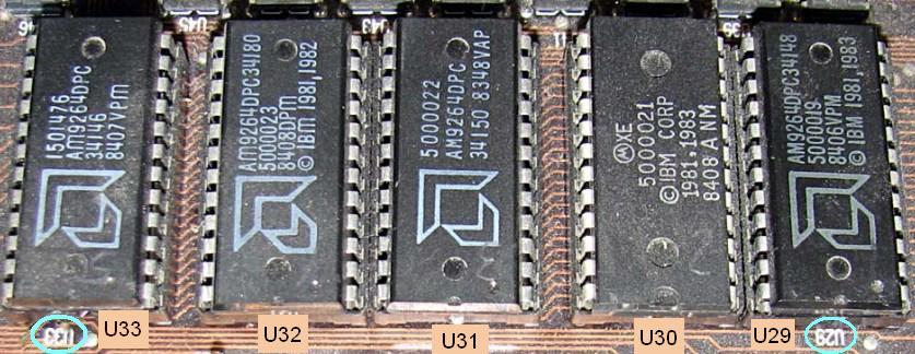
From a 2008 photo, courtesy of Rune Tapper, pc-museum.com. (This
particular IBM 5150 had been "Made in Greenock, Scotland,"
some time after week 8 of 1984, since a number of chips soldered to the board had that
date code; note the '8408' on U30 and U32.)
As noted above, the ROM chip U33 (IBM # 1501476) contains the 3rd version of the 5150 BIOS code. Take this link for photos and details of some ROM chips for all three BIOS versions used in various IBM 5150 models. Take this link for photos of both ROM and EPROM chips in various IBM 5160 machines, and for photos and part numbers of the BIOS chips used in the IBM PC/AT (5170) machines, take this link.
For testing or even small production runs, ![]() PROMs (one time only, Programmable ROM) or
PROMs (one time only, Programmable ROM) or ![]() EPROMs (Erasable Programmable ROM) may
have been used on some early PC Compatibles, since the manufacturer could then test and use revised code and not be left with any ROMs in their stock
having either erroneous or obsolete data. Both PROMs and EPROMs usually have part numbers beginning with 27, but an EPROM has a small quartz window on
top (often covered by a label), so its memory can be erased with a specific high intensity beam of ultra-violet light; allowing it to be reused.
EPROMs (Erasable Programmable ROM) may
have been used on some early PC Compatibles, since the manufacturer could then test and use revised code and not be left with any ROMs in their stock
having either erroneous or obsolete data. Both PROMs and EPROMs usually have part numbers beginning with 27, but an EPROM has a small quartz window on
top (often covered by a label), so its memory can be erased with a specific high intensity beam of ultra-violet light; allowing it to be reused.
Here's a 32-pin DIP BIOS chip from "Award Software, Inc. © 1995" (on a Soltek
SL-52B2 motherboard), with "PCI/PNP 586" and "S/N:034147973" on its label: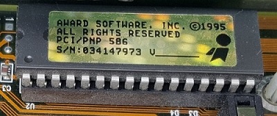
Much later, motherboard manufacturers designed circuitry and utility programs for various types of ![]() EEPROMs
(Electrically Erasable Programmable ROM; part numbers usually begin with a 28 or 29) that allowed users
to reprogram their own PC's BIOS. [This also meant the code could be corrupted if a power-loss occurred during
the upgrade process! Of course, having a known-good battery-backup power supply could prevent that.]
EEPROMs
(Electrically Erasable Programmable ROM; part numbers usually begin with a 28 or 29) that allowed users
to reprogram their own PC's BIOS. [This also meant the code could be corrupted if a power-loss occurred during
the upgrade process! Of course, having a known-good battery-backup power supply could prevent that.]
If the BIOS chip became corrupted, it required purchasing a pre-programmed replacement chip; unless a
user was so unlucky as to find the PC manufacturer had soldered the BIOS chip to the board! Even then, the BIOS chip
generally still had 24 rather large pins, and an electronics hobbyist could disable (or cut away) the old chip and solder the
new one to the existing legs (pins) without having to unsolder the old chip. Of course, if the cost of a programmed chip was
too high, then a better board with more features would win out. The worst class of motherboards in relation to BIOS chips were
those that stored the code in a chip soldered onto the board and also required the user to run an upgrade under Windows,
without anything else running! So, forgetting to disconnect the Network cable or to use TASK MANAGER to kill all but the
essential processes, meant you could easily turn such a motherboard into a useless piece of junk!
PCs with a better design philosophy, had a built-in bootstrap routine that would remain unaltered, thus
allowing users to recover from failed BIOS upgrades. And more recent motherboards, may have a Dual BIOS system[15], so users can re-boot from a secondary BIOS chip that was not in the process of being
changed if a power-loss or some other event occurs. When the PC boots-up again, it will use the secondary BIOS and the user
can go back to reprogramming the primary BIOS chip. Depending upon how the board manufacturer decided to implement their
dual BIOS design, the second chip may be a safety chip that is 'read only' and can never be changed (GIGABYTE's design);
which has the solid advantage of having some BIOS code that could always be relied upon, unless it had a hardware failure too.
Or, a routine may exist to copy the successfully upgraded chip's contents to the other BIOS chip, after determining there is no
problem with the updated code. The BIOS could then check that the copied code matches that of the upgraded chip, before
allowing another upgrade (decidedly more difficult to program and might allow a hacker's code to be your new 'backup code').
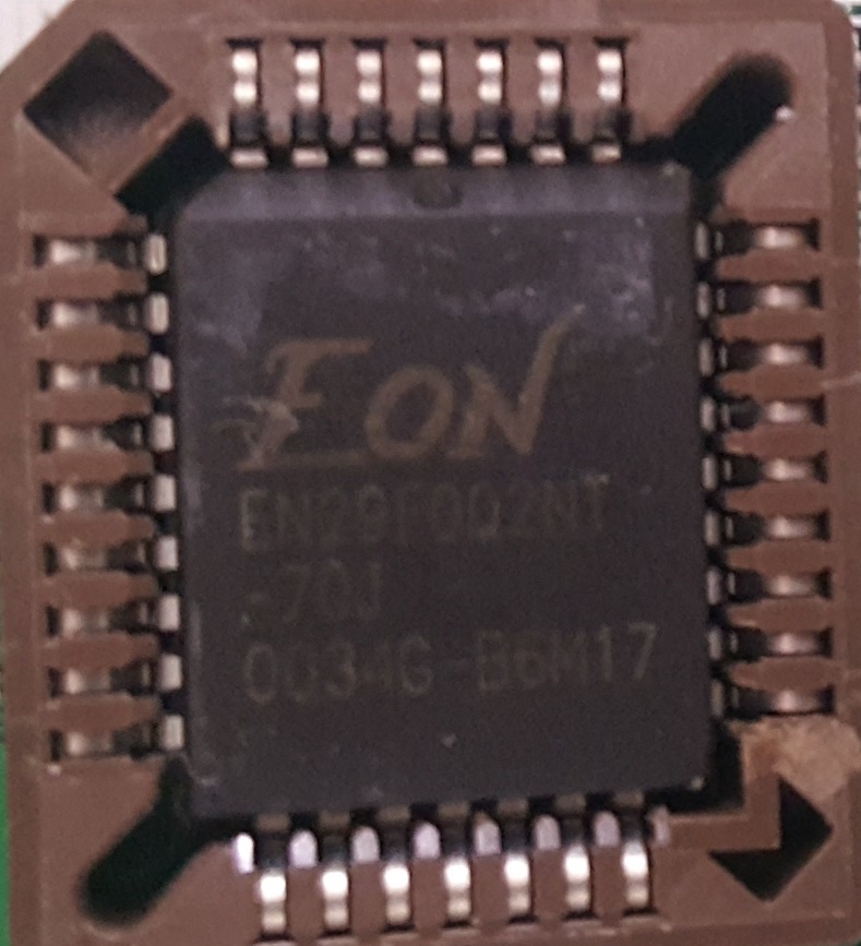
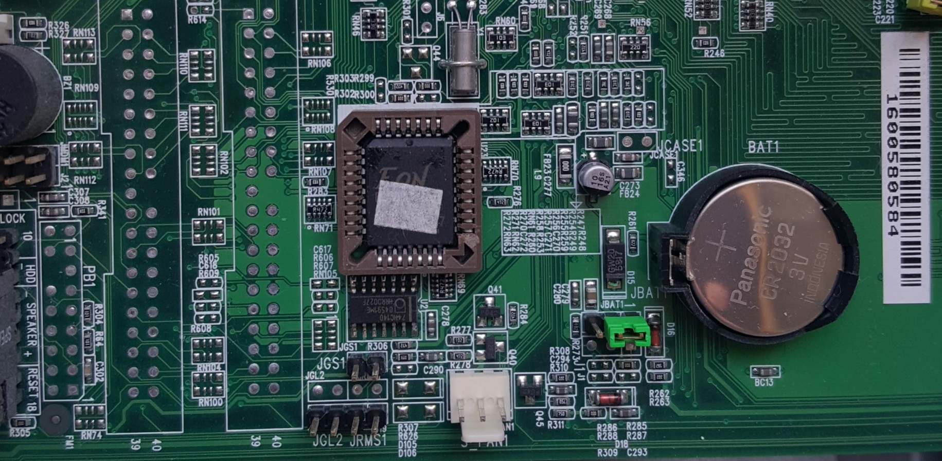
The photos below show a 2 Megabit (or 256 KiB of 8-bit bytes) Flash Memory BIOS chip in a 32-pin PLCC package made by Eon (Eon Silicon Solution, Inc.; part number "EN29F002NT-70J" with an additional line: "0034G - B6M17") on a "Micro-Star" International (MSI) model "MS-6330" "K7T" "Turbo Ver. 3" motherboard:
 |  |
The Dell E521 PC also used a 32-pin PLCC chip (SST 49LF040B 33-4C-NHE; a 4 Megabit chip to store up to 512 KiB of BIOS
code). Pictured ![]() here is an early Gigabyte DualBIOS™ board using two PLCC chips.
here is an early Gigabyte DualBIOS™ board using two PLCC chips.
But eventually, motherboards were designed to use small 8-pin,
![]() Serial Flash BIOS chips
(such as the Macronix™ MX25L8005; an 8 Mbit or 1024 KiB chip, with Boot Lock protection), its code being accessed by the
board's South Bridge (such as Intel's ICH9; I/O Controller Hub 9) using an
Serial Flash BIOS chips
(such as the Macronix™ MX25L8005; an 8 Mbit or 1024 KiB chip, with Boot Lock protection), its code being accessed by the
board's South Bridge (such as Intel's ICH9; I/O Controller Hub 9) using an ![]() SPI bus.
SPI bus.
How to Identify your PC's Chipset
The best source of information, if it's available, would be from the engineers who designed your PC's motherboard.
ASUS™ and GIGABYTE™ both provide manuals online for most of their products; other motherboard companies may as well. A
number of chips on our GIGABYTE boards were listed in these manuals. However, most likely due to the cost of support, most PC
manufacturers do not supply you with such details.
But utility programs also exist which will search PC buses for ID
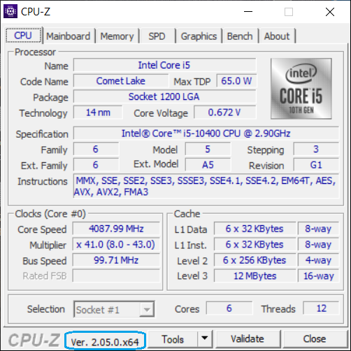
bytes that reveal the identity of a number of its ICs. One which we've used for years is called CPU-Z; available in both 32-
and 64-bit OS versions; both installable and portable downloads:
![]()
![]() CPU-Z
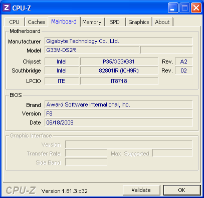
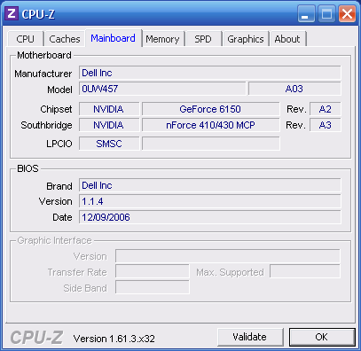
(the last version was 2.05. The program's Mainboard TAB window displays whatever it knows about a PC's chipset and BIOS.
Below you'll see examples for both a Gigabyte Motherboard and a Dell PC. On the left, most of the data is the same as we found in the
manual. However, the data displayed here for the Dell PC (and other name-brand computers) is generally unavailable. Now we at least
know it's using a chipset from NVIDIA, and some kind of Super I/O chip from SMSC ("Standard Microsystems Corporation") for
its LPC (
CPU-Z
(the last version was 2.05. The program's Mainboard TAB window displays whatever it knows about a PC's chipset and BIOS.
Below you'll see examples for both a Gigabyte Motherboard and a Dell PC. On the left, most of the data is the same as we found in the
manual. However, the data displayed here for the Dell PC (and other name-brand computers) is generally unavailable. Now we at least
know it's using a chipset from NVIDIA, and some kind of Super I/O chip from SMSC ("Standard Microsystems Corporation") for
its LPC (![]() Low
Pin Count) I/O bus. We had to examine the board to find it was an SCH55140-NS chip; whereas the Gigabyte board's LPC I/O chip from
ITE shows it was an IT8718. But neither board's actual BIOS chip is listed here. To see more detailed information about your PC, you
could also download
Low
Pin Count) I/O bus. We had to examine the board to find it was an SCH55140-NS chip; whereas the Gigabyte board's LPC I/O chip from
ITE shows it was an IT8718. But neither board's actual BIOS chip is listed here. To see more detailed information about your PC, you
could also download ![]() PC-Wizard (from the same web site). The Hardware section provides information about the Mainboard, BIOS and Chipset;
among many other items. And the data provided by its remaining sections is so detailed, it may overload your brain.
PC-Wizard (from the same web site). The Hardware section provides information about the Mainboard, BIOS and Chipset;
among many other items. And the data provided by its remaining sections is so detailed, it may overload your brain.
 |  |  |
Once you have the Chipset data, you can search a chip manufacturer's site for details on how data in the chip might be accessed; that data can be used by independent utility programmers to show the actual contents of a BIOS chip, as well as by motherboard manufacturers for use in their own BIOS upgrade programs. Some Board manufacturers may even provide a Windows-based utility to make a copy of your BIOS code! [Note: We do not recommend performing a BIOS upgrade, unless you have been assured it will allow your PC to function in some new way you require it to; such as recognizing a larger disk drive, or fixing a problem. We are only pointing out it may be easy to copy the code from your PC's BIOS chip using a software tool; not to use such tools for overwriting BIOS code, without considering the possibility it may become corrupted.] The following shows one such utility running on a PC (we used the PrintScreen key to capture its image; NEVER do this when upgrading!) and added the yellow rectangle and caption:
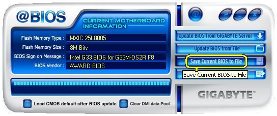 A screen capture of GIGABYTE's @BIOS™ utility running under Microsoft Windows™ XP. | This utility even shows the type of memory
chip being used to store the BIOS code: "MX(IC)25L8005"; as well as its 8 Mbits capacity. Unfortunately, some recent GIGABYTE boards reveal less about the hardware and may not even be able to backup the BIOS to a file! |
Note: For anyone wishing to access the BIOS code on a modern PC - without such a utility, you would first need to know how to use
Intel's ![]() Low Pin Count
Specification and any possible variations in the LPC I/O Interface of the different
Low Pin Count
Specification and any possible variations in the LPC I/O Interface of the different ![]() Super I/O chip manufacturers, and then figure out how to communicate with the actual BIOS chip
itself; which could be an 8-pin or 32-pin flash chip of a different manufacturer as well.
Super I/O chip manufacturers, and then figure out how to communicate with the actual BIOS chip
itself; which could be an 8-pin or 32-pin flash chip of a different manufacturer as well.
The Memory Location of a PC's First Instruction
Virtually every PC, since the very first IBM® Personal Computer produced in 1981, to the latest Intel® or AMD® based PC, has had exactly the same Memory address hard-wired into its CPU as a reference for its first instruction![16] This means every x86 PC's CPU always begins executing machine code instructions from essentially the same location inside its BIOS chip. That address is:
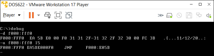
F000:FFF0 (in Segment:Offset notation) or: FFFF0h (in Linear notation). You may also find it represented by FFFF:0000 [See Figure 1 below; as listed in IBM's original Technical Reference manual; P/N 6025008], or as just FFFF:0 (in Normalized Segment:Offset notation). [Read Section 3 of our page on Segment:Offset Addressing to understand why FFFF:0 is equivalent to the Segment:Offset pair F000:FFF0.]
IBM® named this address the "Power On Reset Vector " and it always contains a far jump instruction to the beginning of the BIOS chip's Power-on RESET code. Here's a display of what you'd find in that location and the next 11 bytes of an original IBM® PC's BIOS chip:
Offset: 0 1 2 3 4 5 6 7 8 9 A B C D E F ASCII chars. ------ ----------------------------------------------- ---------------- 0FFFF0 EA 5B E0 00 F0 30 34 2F 32 34 2F 38 31 FF FF EB .[...04/24/81... |
The first five bytes (shown in green ) comprise the Power-On Reset Far Jump. These 5 bytes disassemble to:
JMP F000:E05B
As you can see, Segment F000: is embedded inside this instruction, thus the reason its location is often referenced as F000:FFF0. Although the location of this far jump instruction was essentially 'set in stone' for all early PC BIOS, it's not a requirement that where it jumps to next always be the same; yet every IBM PC BIOS or Clone that we've examined for at least a decade after the IBM 5150 always jumped to "F000:E05B". Exceptions increased as time passed, since any other address could actually be used. For example, in an AMI BIOS we found on an ASRock PC dated "06/15/12" (so 2012), its first instruction is: JMP F000:FFAA which also contained a jump there, and the next instruction was yet another jump!
Of the twelve IBM engineers assigned to create the IBM Personal Computer (model 5150), David J. Bradley[17] developed the code for its BIOS. So he's the one who, among all its other details, decided where in Memory the BIOS would place and execute the code from the first sector of the IBM PC's first floppy diskette's Boot Record. The location he chose was 0x7C00 (or 0000:7C00 in Segment:Offset notation). Unlike the first 'jump address' mentioned above (to F000:E05B), later BIOS authors could not have chosen a different location in Memory for loading the initial bootstrap routines without having their code become incompatible with existing boot diskettes! So IBM (and all the PC-clone companies which followed) continued to use that same location in Memory for their hard disk drive's Master Boot Records (MBRs).
Release Date
The next eight bytes (shown in yellow ) were originally called the "RELEASE MARKER" by IBM; they always contained the release date of the BIOS code (which was 04/24/81 for those first PCs).
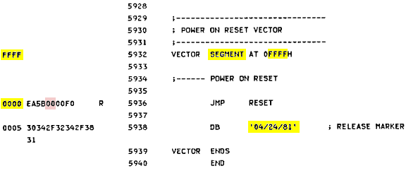 |
| Portion of page A-80, Appendix A, "ROM BIOS Listing," in the
Technical Reference manual (IBM Part Number, 6025008), First Edition (August, 1981), of the IBM Personal Computer Hardware Reference Library. (Click on figure above for larger size.) Figure 1 |
[ In Figure 1, there's an error in the machine
code listing for the location of the Power On RESET code in the "JMP RESET" instruction. This is exactly how the
original "IBM Personal Computer Technical Reference Manual," was printed. This should have been listed as: EA5BE000F0 rather than "EA5B0000F0";
if you check the address shown on page A-5, it's obvious "RESET" begins at the address we've specified.]
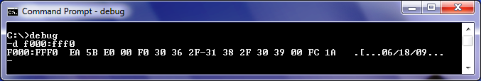
The practice of including "release dates" at this location in BIOS code was continued for every PC Clone BIOS we've examined, and even for many decades to follow inside the DOS compatible modules of later BIOS code. If you install some version of DOS under VMware Player 17 and run the Dump DEBUG command show below, it will show a release date of "11/12/20".
Anyone running a Microsoft/IBM OS from DOS through Windows™ 7 (32-bit), should be able to enter the following DEBUG commands (Windows users must first click on start —> Programs —> Accessories —> Command prompt to open a 'Command Prompt' window. Windows 7 users may be required to select 'Run As Administrator' next to the Command Prompt icon in order to access DEBUG), and obtain results similar to the following (DEBUG.EXE should already be in your path):
C:\>debug |
ENTER the commands shown in green at the DEBUG prompt ("-"). You can see we have the same Jump instruction as the original Personal Computer on this one, but this BIOS code was released on April 14, 2003 ("04/14/03"). (For more on the use of DEBUG, see our Guide to MS-DEBUG).
Here's a Windows™ 7 (32-bit) Command Prompt using DEBUG to show its PC's BIOS release date of "06/18/09":
On early PCs, RAM was an expensive and limited resource that was used as wisely as possible for the the execution of user's programs. Since the original PC could be purchased with only 16 KiB (16 x 1024 bytes = 16,384 bytes) of memory, we know for a fact it would have been impossible to fit the 32 KiB of ROM BASIC code into memory. But using half the available memory for even the 8 KiB of initial bootstrap code made no sense, since it could be accessed from its own ROM chip just as fast as any code in the dynamic RAM chips; both having a 250 nano second access time[18]. Once RAM became much faster than ROM or EEPROM ICs and PCs commonly had many megabytes of memory, system engineers had motive enough to first copy bootstrap routines from the BIOS code into memory, then execute it there. This made it possible for BIOS programmers to explore a number of other advantages to having their code shadowed in RAM; which we'll point out in our next section. But first, we need to mention some methods for making copies of whatever BIOS code still remains in memory after a PC boots up:
How to Save BIOS code from the First 1 MiB of a PC
As we mentioned above, for first generation PCs, BIOS code always had to be read directly from its chip(s).
Not only when the PC was booting-up, but every time a program used a system Interrupt or needed to access any other BIOS
code stored in its ROM (Read Only Memory) chip(s). In those days, the address lines corresponding to the last segment of
memory were hard-wired only to locations within the BIOS chip(s). Later on, PCs were made in which the BIOS code was
first copied into RAM and then used from there instead of directly from the BIOS chip(s).
Motherboard and BIOS chip designs are now much more advanced and vastly different in how they function before even starting
the POST than those early PCs, but it's still possible to examine some of the BIOS code that's copied to the
last 64 KiB and other Segments of a computer's first Binary Megabyte of Memory. Although early PCs often revealed an exact
duplicate of the code from their BIOS chip(s), what you'll find today, for example, on a PC running Windows XP, will only
be a small portion of the full BIOS code that has been copied yet again into a Virtual Memory address space used by the
NTVDM program to simulate the first Megabyte and beyond of a computer's physical memory. Nevertheless, these bytes are
similar to (possibly even the same as) a small section of all the bytes archived in whatever hardware is actually used
to store the PC's BIOS code.
NOTE: The BIOSDUMP program below will not function
under 64-bit Windows 7 or later, since it relies on DEBUG, a 16-bit program!
To make a copy of this code on your own PC, simply download and run our BIOSDUMP Batch program
which includes a DEBUG script file that uses MS-DEBUG to read all the bytes from F0000h to FFFFFh in memory
and write them to the file BIOSDUMP.BIN. Being DEBUG purists, this script file was designed to make sure the first 256 bytes
of DEBUG's memory space would not be altered. (Note: This download also includes VIDEODMP.BAT and a script file for dumping
the C000: segment; the standard location for VGA video BIOS code.) The scripts cause DEBUG to perform a two-step
process that first copies the code to a 65,280-byte file, followed by a 256-byte file. Then the two *.BIN files are combined
using the DOS "COPY /b" command; lastly, the intermediate *.BIN files are deleted.
Instructions for using BIOSDUMP.ZIP: Simply extract all 4 files to a Windows or DOS folder of your
choice, then double-click on one of the *.BAT files, or enter its name at a DOS prompt to run it. The Batch programs run
the associated *.DSF Debug Script so you don't have to type in the DEBUG commands. (If run from a bootable floppy diskette,
make sure a copy of DEBUG.EXE is in the same location or in the path.)
In order to quickly skim through the contents of any *.BIN file created by these programs, or to search for either a text string or hex byte pattern, we recommend using the free hex/disk editor, HxD.
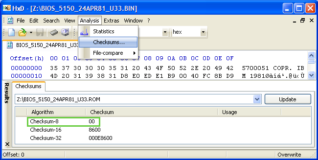
BIOS Checksum Bytes
The last location in an early PC's BIOS chip was called its CHECKSUM byte. It was used to help check
that none of the chip's bytes had become corrupted (changed values). For example, the Checksum Byte of the first IBM
Personal Computer is "EB". This value was computed by first adding together every
preceding byte of the PC's 8 KiB BIOS code, two bytes at a time, keeping only the last 8-bits (one byte) of the sum, and
finally subtracting that value from 100 hex. Thus, the Checksum Byte ensures that running an "8-bit Checksum
operation" on every byte in the BIOS chip will produce a result of zero (0). [ Note: An 8 KiB file full of only FF bytes would also have an 8-bit Checksum of
zero, but its 32-bit Checksum would be 1FE000; which is the sum of all 8,192 of its
bytes added together (2,088,960 decimal).] In summary, an 8-bit Checksum Byte can be computed as follows (we
also show in the table below all checksum data for the original IBM PC's three different BIOS chip versions):
1. When you have finished coding the BIOS, insert a Checksum Byte of 00 (or simply proceed without one).
2. Use a program or utility to compute the 8-bit Checksum of these bytes.
3. Subtract this checksum from 100 hexadecimal; for example, in the table below: 100h - 15h =
EB.
4. The result is the 8-bit Checksum Byte for the BIOS; ensuring its final 8-bit Checksum is zero.
BIOS Checksum Data for U33 of the 5150 IBM® Personal Computer | |||||
ROM Version P/N (Release Date) |
Original Checksum |
Checksum Byte |
Final Checksum |
||
8-Bit |
32-Bit |
8-Bit |
32-Bit |
||
5700051 (04/24/81) |
15 |
E8515 |
EB |
00 |
E8600 |
5700671 (10/19/81) |
65 |
E8565 |
9B |
00 |
E8600 |
1501476 (10/27/82) |
89 |
EAF89 |
77 |
00 |
EB000 |
If you wish to compute the 8-bit (or 16- or 32-bit) Checksum of a file, you can easily do so using HxD, as shown here:
This BIOS file begins with the part number of its programmed ROM chip (5700051) followed by IBM's
copyright phrase ("COPR. IBM 1981") which some have mistaken as an erroneous spelling of 'Corp.'
What Most Can Find Ain't All There Is!
(Or: There's more to modern BIOS code than most have imagined!)
Although you could boot-up your computer with a DOS boot diskette or a CD-ROM disc so there's no chance of its memory being altered by anything but 16-bit real DOS before dumping its contents, even then there's no assurance (without prior research) this will provide you with a copy of all the bytes actually contained in its "BIOS chip(s)". Why? Because the BIOS code may include features that are never retained in memory; for example, a PC company's splash screen that often appears on the display when a computer is first turned on. Or, for example, this familiar EPA ("Energy Star") Logo:
 | This bit-map file had to be converted from a special AWARD BIOS Bit-map file ("AWBM") after extracting it from an LHA compressed file named "AwardBmp.bmp" stored within a PC's actual 128 KiB BIOS chip. |
To see just how sophisticated modern BIOS code has become; using compression and possibly even encrypting its machine code, we've decided to delve into some of the methods used by BIOS manufacturers for our readers. We want you to see how much BIOS code has changed over the decades.
I wrote those words above way back in 2007; roughly two decades ago! You've likely seen in additions I made to this page far above how various features were added as soon as PC Clones with even an Intel 80286 CPU were being produced.
Feel free to write to me about your own PC's BIOS if you have an interest in determining its contents and where its BIOS code is actually stored.
VMWare and The VMWare Legacy BIOS File: BIOS.440.ROM
Completely Replacing the VMWare BIOS File:
This section deals primarily with the use of VMWare's BIOS under a Microsoft Windows OS, but our first example here was
originally created by Pete Batard for VMWare users under a linux OS. However, you can use Pete's VMWare bios.rom file just fine
under any Windows XP, 7, 8, 10 or 11 OS!
1) If you do not already have VMWare installed on your Windows PC, you
can get the FREE VMWare Player 17 (not
Workstation) for Windows 10 from TECHSPOT (or Player 12.5.7 for an older CPU / Windows OS) and also for linux.
2)
First, proceed to Pete's webpage for creating your own
BIOS code to run under VMWare and read the interesting discussion on Pete's blog about the steps required for doing so under
linux and how he made his own BIOS file.
3) Then download the file, vmbios-1.0.tgz, under his
"Goodies" section near the bottom. If you don't know how to extract from a .tgz file, you can use the free 7-Zip to do so! (An absolutely fantastic tool for opening almost any compressed file, even
executables and more which I wrote a bit about here concerning the NTFS File System.)
4) In 7-Zip, open the '.tar' file, and finally extract only the bios.rom file into one of your VMWare virtual machine
folders; actually, I'd recommend creating a new minimal VM titled "SerialPort" (or similar) for testing any new BIOS (such as my
own modified versions below) which will write to a text file in that folder.
5) Inside that VM folder, look for its .vmx file, open it in any plain text editor; such
as Notepad (or Notepad++) and add (insert) the following line (including spaces and quote marks) to that file (the location shouldn't
matter, but I put it about 4 or 5 lines below the top in mine):
bios440.filename = "bios.rom"
6) Be sure to add a serial port to the VM's resources (you can name the text file whatever you want):
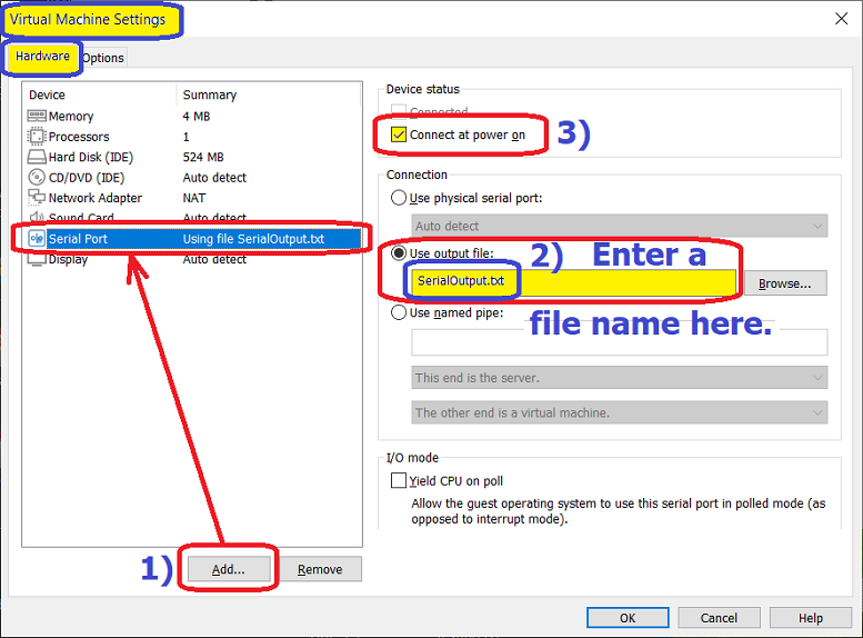
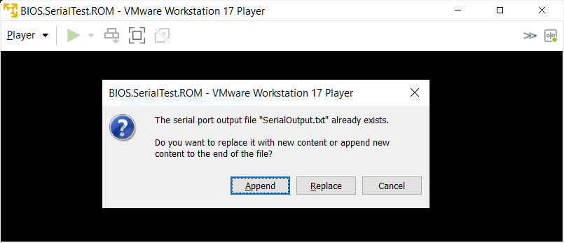
7) Whatever else you have in that VM; such as an HDD with an OS, doesn't matter, since Pete's "bios.rom" code will go into an endless loop after writing to the serial output text file. NOTE: The VM may first ask if you want to "Append" to or "Replace" that file (then you must power off the VM Guest):
Open the file in the VM's folder and you'll see the "Hello BIOS World!" message.
Labwork 1: Modifying Pete's bios.rom File:
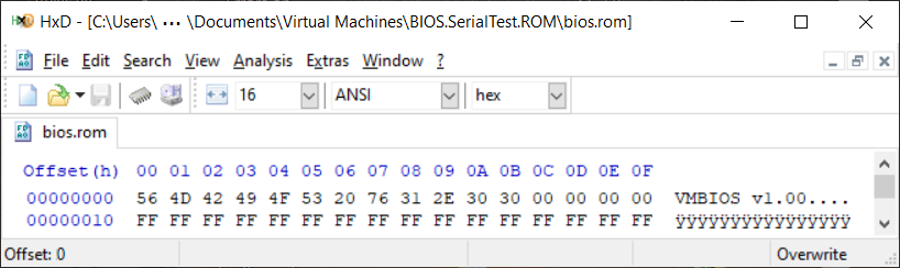
If you open Pete's bios.rom file with a Hex file editor (we of course, recommend using HxD to do so), the first thing you'll see is the ID string he decided to put at the beginning of his file. (If you feel like it, you could change that; it's not code, and it's never checked.)
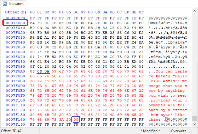
Using whatever hex file editor you prefer, jump to offset 0x7F000 (for HxD, use: CTRL + G then enter 7F000). As shown in the pic below, since Pete's code ends with the ASCII message string (and there's plenty of room for a whole page of text), go ahead and modify the string with whatever you wish to print. But, be sure you include a 0x00 byte at the end:
Save your modified file and run the VM again. Now your message should appear in the serial output file.
Lab 2: Rewriting Pete's Code:
My Windows 10 PC has the latest Microsoft distribution of ubuntu linux installed; along with all the files necessary to assemble (with GNU as) and create a new "bios.rom" file as described on Pete's blog page. I don't expect everyone who reads this page to do that, but you should be able use (and even modify the string in) the bios2.rom file presented here.
BACKGROUND STORY: For some time I'd been interested in adding (injecting) some extra code into VMWare's Legacy BIOS.440.ROM file in order to see which Port 0x80 Diagnostic Codes it would pass through before attempting to locate a bootable OS. After reading Pete's blog, rather than waiting to learn how to use AS and especially LD to create some suitable code for doing so, I simply replaced some of his instructions with NOPs, copied the code 'as is' to a free area, then 'hacked' a number of the jumps using DOS DEBUG until I was able to get it to spit out a message each time the BIOS code executed an OUT 0x80 instruction.
I'm hopeful that others can learn some things from my slight revision of Pete's code (see bios2.S in the Zip file) as well as how to set a specific location in a .ROM file for execution to jump to! The attached bios2.ld file shows that in order to have execution jump to F000:D500 (offset 0x7D500 in the included bios2.rom file), it was only necessary to change the line beginning with "main_address = " to: main_address = 4096M - 11008; (the "11008" was arrived at by solving: 10000h - 0D500h or: 65,536 - 54,528 = 11,008); the value is straight decimal bytes without any M or K suffix. Download the BIOS2.ZIP file, put the bios2.rom file in your test folder, make sure to edit the .vmx file for the new .ROM file, run the VM and note this code executes as if it were the same; with only a change in its message. Instead of using two 32-bit SHIFT instructions, this .ROM file uses all 16-bit code. I've also included in the ZIP file a disassembly of the code using DOS DEBUG to prove that point.
Modifying (Injecting Code Into) the VMWare BIOS.440.ROM File:
This section will provide you with everything necessary to understand how to inject some code into the official VMWare BIOS and the reason why I did so: Since the BIOS code runs as an emulation under an already existing OS, there is no possible way to connect a hardware diagnostic card to a PCI bus in order to obtain any possible diagnostic codes. The question being: Was there even such a routine in the BIOS code; or was it a very 'stripped down' version that could never be used with an actual motherboard?
First Step: Locate a copy of the official "BIOS.440.ROM" file. If you have a rather old version of VMWare
Player (or Workstation); such as version 6 or 7, then you should be able to find the following "6006" file here:
C:\Program Files\VMware\.rsrc\BINRES\6006 (The file size will be 512 KiB; exactly 524,288 bytes, and under VMWare 7.1.4
build-385536, the file was dated "March 26, 2011, 12:41 AM".) For those who've downloaded and installed a fairly recent VMWare
Player (versions 16 or 17, for example), you can simply search your system for "BIOS.440.ROM" (using a search tool such as
Everything), but you might find it here:
C:\Program Files (x86)\VMware\VMware Workstation\x64\BIOS.440.ROM (along with a number of other .ROM files). No matter
which file you obtain; either a "6006," or a .ROM, nor what the file's date is, the contents will always be the same! The
BIOS file will have these hash values:
MD5: 88A6E1E0706B8669FF962A22CADBB974
SHA1: 4DEF8FFE004164C8D3EDDF6E921CEF0F7BB7C22B
SHA256: 77416D8CBF98B6DBF68D9AA68222A1D2B8C51D6BAA47AAFE62F5216B41F239B0
Getting to Know the File:
Who made this code?
At offsets 0x74280 through 0x742CD you'll find: "PhoenixBIOS 4.0 Release 6.0" and "Copyright 1985-2001 Phoenix Technologies
Ltd." which indicates the code must have originated with Phoenix Technologies, but there's also the string "Copyright 2000-2020 VMware,
Inc." (at offsets 0x7348B and following) showing that at least some changes were made specifically for WMware which allowed them to copyright
the code. I can't help wondering if the file's copyright expired a couple years ago? Does anyone know for sure? A couple other strings of interest
would be: "Intel Corporation" and "440BX Desktop Reference Platform" (indicating the code was created for the Intel 440 BX
chipset among other possible hardware specifics). In fact, VMware has been telling everyone for years that their VM's emulate the following
hardware:[19]
• Intel 440BX-based motherboard
• NS338 SIO chipset = PC97338 Super I/O compliant chips
• 82093AA I/O Advanced Programmable Controller (I/O APIC)
• Phoenix BIOS 4.0 Release 6 with VESA (video display) BIOS
I added the Super I/O compliance above, since the tests with Pete Batard's code showed that their means of communicating across Serial
COM ports (listed as a National Semiconductor NS338 Super I/O chip) must be compliant with the more general data sheet he referenced as
PC97338.
Some Recommendations: To further your understanding (though not strictly necessary), unless you have
access to a working Windows XP machine, I'd highly recommend setting up a VMware Player VM of Win XP (SP-3) OS in order to use 16-bit Apps
which are impossible to run under a 64-bit Win OS; this will also allow you to use DOS DEBUG in a
Command window. HOWEVER (and especially for dealing with any 32-bit instructions you will encounter in the BIOS.440.ROM file), I'd highly recommend
adding Enhanced DEBUG to your tools; though it may have some quirks compared to the
original DEBUG in some cases, so I wouldn't consider it a fully compatible replacement. An even better way to examine the machine code found
in this file would be to dynamically execute what you can under The Bochs (GUI) Enhanced
Debugger (Bochs does not emulate the same hardware that VMware does, so this BIOS code will fail at some point when run as its
BIOS; you would need to replace the existing "romimage:" line in its .bxrc file with: "romimage:
file="BIOS.440.ROM", address=0xfff80000, options=none # 512k at memory top" - what follows the # sign is a comment).
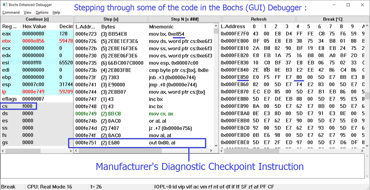
The Serendipitous Location of one "E9 00 00" Near Jump: If you search the file for all the instances of
"E9 00 00," you'll find over 50 of them! But for our Code Injection Example, the only bytes we are interested in are found at offset 0x7E753 because they follow what can be called a motherboard manufacturer's Diagnostic Checkpoint (that is, the x86 Assembly
instruction: OUT 0x80, AL) which sends a chosen Hexadecimal Code out Port 80h. But there is no physical bus to connect a POST (Diagnostic) Card to, so what can we do? Yes, inject our own
routine into the BIOS code that will send those diagnostic codes out a SERIAL PORT instead!
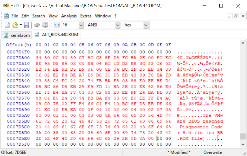
More Details: Of the whole 512 KiB contents of the BIOS.440.ROM file, only the last 16 KiB comprises what's know as the "Boot
Block" (labeled by Phoenix the BB.ROM file when the whole thing is separated into its individual components), and the first 5,802 bytes
of BB.ROM are likely unused padding of zero bytes (from offsets 0x7C000 to possibly 0x7D6A9). This is one of the reasons I chose to inject my code
into offsets 0x7D500 and following (over 416 bytes available; leaving more than enough room for my strings, and also because "D5" looks
like my initials; ;-) ). To find the correct bytes for a 3-byte backwards JMP to offset 0x0D500, DEBUG (or Enhanced DEBUG) users would simply open
DEBUG and enter (GREEN indicating what to enter at DEBUG prompt; Yellow xxxx's would be whatever initial working segment the OS assigned):
-a e753
xxxx:E753 jmp d500
xxxx:E756  [Just press ENTER key here!]
-u e753 e755
xxxx:E753 E9AAED            JMP     D500
---- |
So, we'll need to change the hex bytes at 0x7E753 from "E9 00 00" to: "E9 AA ED". For those without DEBUG, the bytes are calculated as follows: E753h - D500h = 1253h, but the difference must begin after the 3 bytes of the jump itself, so we get: 1256h. Then, because this is a relative reverse jump (forward jumps use "0000" through "7FFF" and reverse jumps the negative signed values of "FFFF" through "8000"), the 2's compliment of that difference must calculated (2's compliment means inverting every bit, or performing a logical NOT on it, and then adding 1): So, 1256h --> EDA9h + 1 = EDAAh. And as with all x86 machine code, hex values are stored "little endian" so the order must be: "E9 AA ED" (Note: This page on Two-Byte Jumps has 2's compliment examples for SHORT jumps).
Lab 3: Injecting Code Into and Running a VM with the Modified BIOS.440.ROM File
First Edit of the BIOS.440.ROM File: The reasons for doing this were explained in detail above! First, make a copy of the VMware file BIOS.440.ROM (I'm using "ALT_BIOS.440.ROM" here) and place it into one of your VMware Virtual Machine folders. Open that file in a hex editor, move the cursor to offset 0x7E754 in the file, change the two bytes as shown in RED in the figure below (to: AA ED) and save the file: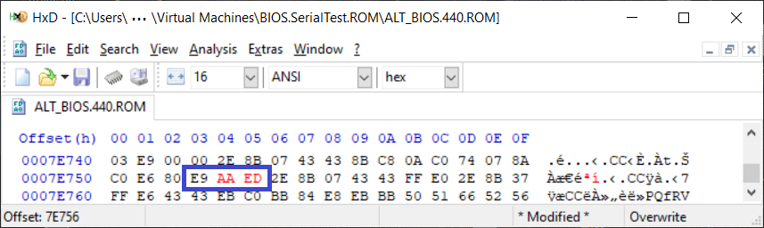
Creating the Code:
The first time I wrote out this code I made use of MASM 6.15 under a Windows XP VM. I've
made it available here for anyone interested (but it required using a bunch of NOPs that had to be edited
after a .COM file was assembled). So, I've written a linux Assembly file (serial.S) which I'll include with another .ld file and the .ROM
output file below. DESCRIPTION: First, this code preserves the AL byte which the original Phoenix BIOS code would send OUT Port 80h, but I had to
do a little manipulation on it (making it ASCII instead of Hex) before saving it in the DI Register. The rest of the code loops through many of the same
assembly instructions you saw in Pete Batard's code, but TWICE, because I added some instructions to print out that Diagnostic Code value in between. And
of course, the code to return back to the original execution sequence in the VMware BIOS code replaces Pete's endless loop code!
Second Edit: Having made a JMP to location 0x7D500 in your ALT_BIOS.440.ROM file, now it's time to overwrite (not insert) the bytes
at that location with the ROM code you'll find (or create yourself from the assembly files) in this ZIP
file. [ Update: Though not actually necessary, for any future Assembly coders, I revised my Hex to ASCII "hack" with code
that converts the low-end Hex digit (A-F included) to ASCII in this revised serial.S file. Simply
substitute this serial.S file for the one in the previous download, or use the bytes found in the other file (serial.rom.bin) to modify ALT_BIOS.440.ROM; this code is technically 3 bytes longer than the previous ROM output file, but since the
BIOS.440.ROM file is zero-byte 'padded' you don't need to copy and write the last byte.]
This file
has a lot in it: serial.S, the Assembly file for creating the code under linux; serial.ld, the linux LINKER file
which is a necessary part; Makefile, the file linux uses when you enter "make" at a folder prompt with
those 3 files in it, to create the output files! Then, serial.rom, the file my version of linux made from them, as well as a copy of
masm6_serial.com, the binary MASM 6.15 made from the MASM 6 Assembly file I linked to above; MASM6_CODE.txt and
SERIAL_CODE.txt, which allow you to compare the actual machine code bytes both of those assemblers used. Since the VMware BIOS file
is likely still copyrighted, you'll need to finish editing it using the included serial.rom file. This will require a Hex Editor that can
copy hex bytes from one file and then write them into another file (without changing its size; most can do this). The bytes we need to copy are located
offsets 0x7D500 through 0x7D5ED in the serial.rom file; copy those bytes. Open your ALT_BIOS.440.ROM file and set the cursor at offset 0x7D500,
and if you're using HxD, select "Edit" and then "Paste Write" (not 'Insert'). Here's what it should look like at that point:
[ Update: For those who might like some code which is capable of converting any Diagnostic Code from 0x00 to 0xFF into ASCII, you can download serial3.S (and associated files); as before, you can overwrite the BIOS file at offsets 0x7D500 and following with the bytes you'll find in serial3.rom.]
Write those bytes to the file, be sure you have the line bios440.filename = "ALT_BIOS.440.ROM" (or whatever filename
you decided to call it) in the VM's .vmx file, and proceed to test it out. After acknowledging whether you want to replace or append to whatever
file you created for the Serial output, unlike the previous ROMs, which stopped dead, this code should continue to where it doesn't find an OS or boots up
whatever OS you may have already installed in your VM folder. Now look in the folder and open that Serial port textfile. What do you see?
When I tested the first version of my code (not the one you have now), I had to ask, "Why did it stop there?" I already knew how far I
could go when running the BIOS under Bochs, and expected it would provide many more checkpoints, but it didn't! And the more I examine this
VMware BIOS (and hear from others), it seems to be splotches of separated code modules that might never boot an actual motherboard without connecting
more of the code together. I don't have enough factual data to actually make this claim, but it almost seems as if the VMware executable code is overseeing
whether the BIOS should or should not execute certain modules or carry out certain tests. I do know that at one time the minds working on Coreboot
finally decided it wasn't possible to create a useful BIOS ROM for VMware. And recently, I found out there's a section of code in the BIOS ROM made
specifically for communicating with VMware binaries while a VM is running; here's a security article
where you can read more about that (and yes, I verified those instructions do exist in the BIOS.440.ROM file).
For Lab 4 below, we highly recommend reading our page on: Downloading, Installing and Using the IDA 7 Free Version to examine BIOS (and other) files!
Lab 4: Not Everything is Code:
Yes, you already know there are some 'Strings' in the BIOS.440.ROM file, but apart from those, it's quite possible for a number of hex bytes (that one could attempt to disassemble as code) to be Data! As an example of such occurrences, search the VMware BIOS file from offsets 0x7E854 through 0x7E8E9, then answer the question: Do you see any kind of pattern? (Hint: In the "Initial Code" link I provided above, you might recall seeing the hex value "E854" before.) If necessary, spend some more time observing the bytes, then try answering this question (with an additional hint): This whole section is basically a Table of Jump Addresses associated with what code you've already seen?
Coreboot (How to Create a UEFI ROM File and Run one under Qemu)
In the Near Future — I'd be happy to email anyone about this!
Footnotes
1[Return to Text] Although many still refer to the UEFI (Unified Extensible Firmware Interface) code of a modern computer as its BIOS, that would be incorrect! In fact, most current versions of UEFI code contain some kind of legacy BIOS code as a module within their full contents which allows a computer to boot into a Legacy BIOS mode (its CSM — Compatibility Support Module) instead of the normal UEFI boot code. This most often needs to be configured inside the running UEFI user interface, a restart of the computer then being required, before it can boot as if it had only BIOS code installed. In this way, a modern PC might still be able to boot into some version of a DOS only operating system (compatible video drivers may be required).
2[Return to Text] Near the top of the file,
BDOS.PLM (inside the file "cpm_plm.zip"; which can be downloaded from cpm.z80.de), Gary wrote:
C P / M   B A S I C   I / O    S Y S T E M    (B I O S)
                    COPYRIGHT (C) GARY A. KILDALL
                             JUNE, 1975
3[Return to Text] Herb Johnson, owner of the website, retrotechnology.net (which contains a very well documented history of all things pertaining to Gary Kildall, CP/M and DRI), has the following quote by Ken Bergett, formerly of Intel, on this page about the ISIS OS: "Gary did manage to get one of the early production MDS 800 systems, with the disk controller we built for the ISIS project, trading for something Marketing wanted done, and the development of CP/M proceeded in parallel with our work on ISIS. Gary and I discussed possible solutions for doing file allocation and I/O, and how to manage the disk controller, and such like, but each DOS was developed separately."
4[Return to Text] It must be noted here: Although the Intel 80286 CPU was capable of addressing up to 16 MiB of Memory, since neither IBM nor Microsoft DOS used anything above 640 KiB (referred to as "Conventional Memory"), the IBM PC/AT (model 5170; August 1984) came with a maximum of only 512 KiB of Memory on its motherboard. Much later, MS-DOS included EMM386 (for making use of "Upper Memory" — or UMA, that area of Memory above 640 KiB but below 1 MiB) and HIMEM.SYS (a device driver for storing data in Extended Memory). However, Intel™ in April 1985 (and later other companies, such as AST Research) began making ISA expansion boards in April 1985, such as their Above Board (to access what Intel and Lotus called Expanded Memory), which allowed users to add Megabytes of memory to their 80286 PC/AT or Clone computers. So, 3rd party software companies created utilities for using more memory as well. Yet, in October of the same year that Intel was providing more Memory for PC/AT users, they already announced their 32-bit 80386 (or i386) CPU; which would be capable of addressing 4 Gigabytes of Memory! This Timeline of DOS provides a nice glimpse of all the important improvements made for PCs during that era (1980 to 1995).
5[Return to Text] On page 8 of the ASUS® CUSL2-C, Intel® 815EP ATX Motherboard, USER'S MANUAL, Revision 1.04 E639, Copyright ©2000 by ASUSTeK Computer Inc., it states: "Equipped with three Dual Inline Memory Module (DIMM) sockets to support PC100/PC133-compliant SDRAMs (available in 64, 128, 256, 512MB densities) up to 512 MB." [Emphasis ours.] Note: The Black Pearl Edition (CUSL2-CBP) was no different; its User Manual has the same note on page 12.
6[Return to Text] On page 9 of the Intel® 815 Chipset Family:, 82815EP and 82815P, Memory Controller Hub (MCH), March 2001, Document Reference Number: 290693-002, Copyright © 2000,2001 Intel Corporation, under "Integrated SDRAM Controller" it lists: "32 MB to 512 MB using 16Mb/64Mb/128Mb/256Mb technology". And on page 50, it quite clearly states: "The maximum supported main memory capacity is 512 MB." [Emphasis ours.]
7[Return to Text] On page 12 of the GA-G33M-DS2R/, GA-G33M-S2, LGA775 socket motherboard for Intel® Core™ processor family/, Intel® Pentium® processor family/Intel® Celeron® processor family, User's Manual, Rev. 1003, 12ME-G33MD2R-1003R, ©2007 by GIGABYTE™ you'll find: "4 x 1.8V DDR2 DIMM sockets supporting up to 8 GB of system memory." [Emphasis ours.] The fact that GIGABYTE included four sockets on this board, means we'll only need to purchase DIMMs of 2 GB each when moving from a 32 to 64-bit OS to take full advantage of that 8 GiB of memory.
8[Return to Text] On page 28 of the Intel® 3 Series Express Chipset, Family, Datasheet, - For the Intel® 82Q35, 82Q33, 82G33 Graphics and Memory Controller Hub (GMCH) and Intel® 82P35 Memory Controller Hub (MCH), August 2007, you'll find: "Using 1 Gb device technologies, the largest memory capacity possible is 8 GB, assuming Dual Channel Mode with four x8 double sided un-buffered non-ECC DIMM memory configuration.." [Emphasis ours.] And on page 17: "Supports 1-Gb, 512-Mb DDR2 or DDR3 technologies, for x8 and x16 devices, 8 GB maximum memory." [Emphasis ours.]
9[Return to Text] Material will be added here at a later date.
12[Return to Text] For anyone who actually needs to do this, or for those simply curious about how one would go about doing so, it should be noted that the very useful PC technician and forensic investigator's commerical product, WinHex actually has a tool for doing this very thing built into its menu system: Simply click on Tools —> File Tools —> Unify —> Bytewise (8-bit) and the diaglog boxes which pop-up will ask for the two source files and then a name for the output file it should create. Be sure to choose the file from the U27 (or "even" or sometimes "[0]") chip first.
13[Return to Text] From the Phoenix Technical Reference Series book: System BIOS for IBM® PCs, Compatibles, and EISA Computers, Second Edition. The Complete Guide to ROM-Based System Software (Copyright©1991, 1990, 1989, 1988, 1987 by Phoenix Technologies Ltd.), Glossary, page 343.
14[Return to Text] Ibid., page 340.
15[Return to
Text] See this link for how the motherboard manufacturer, GIGABYTE®, explains their ![]() DualBIOS™ system.
DualBIOS™ system.
16[Return to Text] Technically, this has not been exactly true for a very long time. Starting all the way back with the Intel 80286 CPU, the BIOS chip containing the PC's first instruction was no longer accessed at physical memory address 0xFFFF0 (close to 1 MiB), but rather an address line near the top of 16 MiB. The Intel 80286 Hardware Reference Manual, 1987, on page 3-65, under the section "Initializing the 80286 Processor," states:
The 80286 RESET input provides an orderly way to start or restart a system. When the processor detects the positive-going edge of a pulse on RESET, it terminates all activities until the signal goes low, at which time it initializes the CPU to a known internal state; the CPU then begins fetching instructions from absolute address FFFFF0H.
That address is only 16 bytes below 16 MiB. This should raise a question in your mind similar to this one: "How does code at that high of a memory location become the same as the 0xFFFF0 20-bit address under the first IBM PC's Intel 8088 processor?" Well, on page 3-67, the Manual continues with:
The RESET signal initializes the CPU in Real-Address mode, with the CS
base register containing FF0000H and IP containing FFF0H. The first instruction fetch cycle following reset will be from the
physical address formed by these two registers, i.e., from address FFFFF0H. This location will normally contain a JMP instruction to
the actual beginning of the system bootstrap program.
For 80286 systems to operate in Protected Virtual-Address mode, the
80286 (executing in Real-Address mode) must enter Protected mode as part of the software initialization routine.
To accommodate an 80286 operating in both Real-Address mode and Protected mode, the EPROMs containing the system bootstrap
program must answer to both a 20-bit and a 24-bit physical address.
In Real-Address mode, the system
bootstrap EPROMs must respond to addresses in the available 1-Megabyte address space (ignoring the upper four address bits). In
Protected mode, these same EPROMs typically respond to addresses only in the top megabyte of the available 16-Megabyte address space
(using the full 24-bit address).
Figure 3-68 shows a circuit that permits this type of operation by generating one of the
terms in the address-decode logic selecting the bootstrap EPROMs. This term inhibits the decoding of A23-A20 after RESET, when the
system runs in Real-Address mode. After entering Protected mode, the bootstrap program must strobe the [not] PROTMODE signal to
allow full use of the available 16-Megabyte address space.
One source
for the 80286 Hardware Reference Manual.
And with the introduction of the Intel i386 CPU (and applicable to all later x86 CPUs), the BIOS chip's first
instruction is actually accessed through address 0xFFFFFFF0. This is just 16 bytes below 4 GiB.
From the Intel 80386, Programmer's Reference Manual, 1986, on page 176 (of 421), under Section 10.2.3
"First Instructions," we find:
After RESET, address lines A{31-20} are automatically asserted for instruction fetches. This fact, together with the initial values of CS:IP, causes instruction execution to begin at physical address FFFFFFF0H. Near (intrasegment) forms of control transfer instructions may be used to pass control to other addresses in the upper 64K bytes of the address space. The first far (intersegment) JMP or CALL instruction causes A{31-20} to drop low, and the 80386 continues executing instructions [as if they were] in the lower one megabyte of physical memory. This automatic assertion of address lines A{31-20} allows systems designers to use a ROM at the high end of the address space to initialize the system.
We will have a lot more to say about this in the future, and hope to provide a much clearer explanation using our own memory diagrams, so everyone can understand the process. [Return to Text]
17[Return to Text] References: Article on ![]() David J. Bradley in Wikipedia.
David J. Bradley in Wikipedia.
18[Return to Text] "The ROM is packaged in 24-pin modules and has an access time of 250 ns and a cycle time of 350 ns. .... All memory is parity-checked and consists of 16 K by 1 bit or (64 K by 1 bit) chips with an access time of 250 ns and a cycle time of 410 ns." Page 1-5, "Section 1: Hardware," IBM Personal Computer Technical Reference manual, Revised Edition (April, 1983), of the IBM® Personal Computer Hardware Reference Library.
19[Return to Text] Source: Virtual Machine Chipset and BIOS Support.